

Materials and Processing for Advanced Semiconductor Packaging Market Outlook
The Materials and Processing for Advanced Semiconductor Packaging market size was valued at USD $23 Billion in 2025 and is anticipated to reach USD $40 Billion by 2035, growing at a CAGR of 5.7% during the forecast period according to Strategic Packaging Insights.
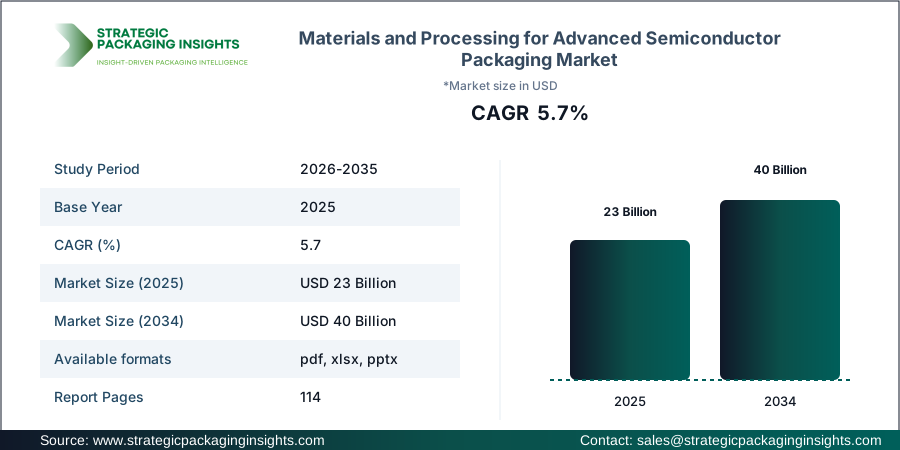
The primary driver of this growth is the increasing demand for advanced semiconductor packaging solutions in consumer electronics and high-performance computing applications. The proliferation of AI and IoT devices, coupled with the need for miniaturization and enhanced performance, is pushing the boundaries of semiconductor packaging technologies. Companies like TSMC and Intel are investing heavily in R&D to develop innovative packaging solutions that meet these evolving demands.
Report Scope
| Attributes | Details |
| Report Title | Materials and Processing for Advanced Semiconductor Packaging Market Projected to Scale to 40 Billion by 2035, Assesses Strategic Packaging Insights |
| By material type | Organic Substrates, Ceramic Substrates, Silicon Wafers, Metal Substrates, Redistribution Layer Materials, Bonding Materials, Encapsulants, Underfill Materials, Die Attach Materials, Molding Compounds |
| By processing technology | Lithography, Bonding and Interconnection, Wafer Processing, Die Preparation, Molding, Encapsulation, Thin Film Deposition, Etching, Plating |
| By packaging technology | Flip Chip, 2.5D IC Packaging, 3D IC Packaging, Fan-Out Wafer-Level Packaging, Wafer-Level Packaging, System-in-Package, Chiplet Packaging, Hybrid Bonding |
| By application | Consumer Electronics, Data Centers, High Performance Computing, Artificial Intelligence, Automotive, Telecommunications, Industrial Electronics, Healthcare Electronics |
| By region | North America, Europe, Asia Pacific, Latin America, Middle East and Africa |
| Base Year | 2025 |
| Historic Period | 2018-2024 |
| Forecast Period | 2026-2035 |
| Number of Pages | 114 |
| Customization Available | Yes* |
Market Trends Analysis
One of the major trends in the Materials and Processing for Advanced Semiconductor Packaging market is the shift towards more integrated and compact packaging solutions. This trend is driven by the need for higher performance and efficiency in consumer electronics and data centers. The adoption of 3D IC packaging and system-in-package technologies is increasing as they offer significant advantages in terms of space-saving and performance enhancement. Companies are focusing on developing advanced materials and processing technologies to support these packaging innovations.
Another significant trend is the growing emphasis on sustainability and environmental impact reduction in semiconductor packaging. Manufacturers are exploring eco-friendly materials and processes to minimize waste and energy consumption. The integration of advanced recycling technologies and the use of biodegradable materials are gaining traction. This shift is not only driven by regulatory pressures but also by consumer demand for greener products. As a result, companies are investing in sustainable packaging solutions to enhance their market competitiveness.
Industry Transformation Analysis
The semiconductor packaging industry is undergoing a transformation with the integration of advanced technologies such as AI and machine learning in manufacturing processes. These technologies are enhancing operational efficiency and reducing production costs. The adoption of automation and robotics in packaging lines is also increasing, leading to faster production cycles and improved quality control. This transformation is enabling companies to meet the growing demand for advanced packaging solutions more effectively.
Additionally, the industry is witnessing a shift towards localized production to mitigate supply chain disruptions and reduce dependency on specific regions. Companies are expanding their manufacturing facilities in key markets such as Asia Pacific and North America to ensure a steady supply of materials and components. This localization strategy is also helping companies to better serve regional markets and respond quickly to changing customer demands.
Trends & Disruptions Impacting Customers' Customers
Downstream customers, particularly in the consumer electronics and automotive sectors, are increasingly demanding more compact and efficient semiconductor packaging solutions. The rise of electric vehicles and smart devices is driving the need for advanced packaging technologies that can support higher power densities and improved thermal management. This demand is influencing semiconductor manufacturers to innovate and develop new materials and processing techniques to meet these requirements.
As downstream customers prioritize sustainability, there is a growing expectation for semiconductor packaging solutions that are environmentally friendly. This shift is prompting manufacturers to explore biodegradable materials and energy-efficient processes. The focus on sustainability is also leading to increased collaboration between semiconductor companies and their customers to develop packaging solutions that align with environmental goals. This trend is creating new opportunities for innovation and differentiation in the market.
Materials and Processing for Advanced Semiconductor Packaging Market Ecosystem
The ecosystem of the Materials and Processing for Advanced Semiconductor Packaging market is complex, involving multiple stages from raw material procurement to end-use applications. The value chain begins with the sourcing of essential materials such as silicon and metals, which are crucial for substrate and component manufacturing. These materials are then processed using advanced technologies like lithography and etching to create high-performance packaging solutions.
Substrate production is a critical stage in the ecosystem, where organic, ceramic, and metal substrates are manufactured to meet the specific requirements of different packaging technologies. The processed substrates are then integrated into various packaging solutions such as flip chip and 3D IC, which are used in a wide range of applications including consumer electronics and automotive. The ecosystem is highly dependent on the seamless flow of materials and technologies across different stages to ensure the efficient production of advanced semiconductor packaging solutions.
Analyst Perspective
Analyst Perspective: The Materials and Processing for Advanced Semiconductor Packaging market is poised for significant growth, driven by the increasing demand for high-performance and compact packaging solutions in consumer electronics and automotive sectors.
The most important structural change in the market is the shift towards more integrated and sustainable packaging solutions. This change is driven by the need for higher efficiency and reduced environmental impact, which is influencing companies to invest in advanced materials and processing technologies.
Companies, investors, and suppliers should closely monitor the developments in 3D IC packaging and system-in-package technologies, as these are expected to drive future growth and innovation in the market. The focus on sustainability and localization strategies will also play a crucial role in shaping the competitive landscape.
Opportunities & Threats
The Materials and Processing for Advanced Semiconductor Packaging market presents significant opportunities for growth, particularly in the development of advanced packaging technologies such as 3D IC and system-in-package. These technologies offer enhanced performance and efficiency, making them highly attractive for applications in consumer electronics and high-performance computing. Companies that invest in R&D to innovate and improve these technologies are likely to gain a competitive edge in the market.
Another opportunity lies in the growing demand for sustainable packaging solutions. As environmental concerns continue to rise, there is an increasing need for eco-friendly materials and processes in semiconductor packaging. Companies that can offer sustainable solutions are likely to attract more customers and expand their market share. This trend is also supported by regulatory pressures and consumer demand for greener products.
However, the market also faces several threats, including the volatility of raw material prices. The semiconductor packaging industry relies heavily on materials such as silicon and metals, which are subject to price fluctuations. This volatility can impact production costs and profit margins, posing a challenge for manufacturers. Companies need to develop strategies to mitigate these risks and ensure a stable supply of materials.
Another threat is the increasing competition in the market. As more companies enter the semiconductor packaging industry, the competition for market share intensifies. This competition can lead to pricing pressures and reduced profit margins. Companies need to differentiate themselves through innovation and quality to maintain their competitive position in the market.
Drivers & Challenges
The primary driver of the Materials and Processing for Advanced Semiconductor Packaging market is the increasing demand for high-performance and compact packaging solutions. The proliferation of AI and IoT devices, coupled with the need for miniaturization and enhanced performance, is pushing the boundaries of semiconductor packaging technologies. Companies like TSMC and Intel are investing heavily in R&D to develop innovative packaging solutions that meet these evolving demands.
Another significant driver is the growing emphasis on sustainability and environmental impact reduction in semiconductor packaging. Manufacturers are exploring eco-friendly materials and processes to minimize waste and energy consumption. The integration of advanced recycling technologies and the use of biodegradable materials are gaining traction. This shift is not only driven by regulatory pressures but also by consumer demand for greener products.
Despite these drivers, the market faces several challenges, including the complexity of developing advanced packaging technologies. The integration of new materials and processes requires significant investment in R&D and manufacturing capabilities. Additionally, the volatility of raw material prices and the increasing competition in the market pose challenges for manufacturers. Companies need to develop strategies to mitigate these risks and ensure a stable supply of materials.
Market Share Analysis
The Materials and Processing for Advanced Semiconductor Packaging market is characterized by a competitive landscape with several key players dominating the market. Companies like TSMC, Intel, and Samsung Electronics hold significant market shares due to their extensive R&D capabilities and advanced packaging technologies. These companies are continuously investing in innovation to maintain their competitive edge and meet the evolving demands of the market.
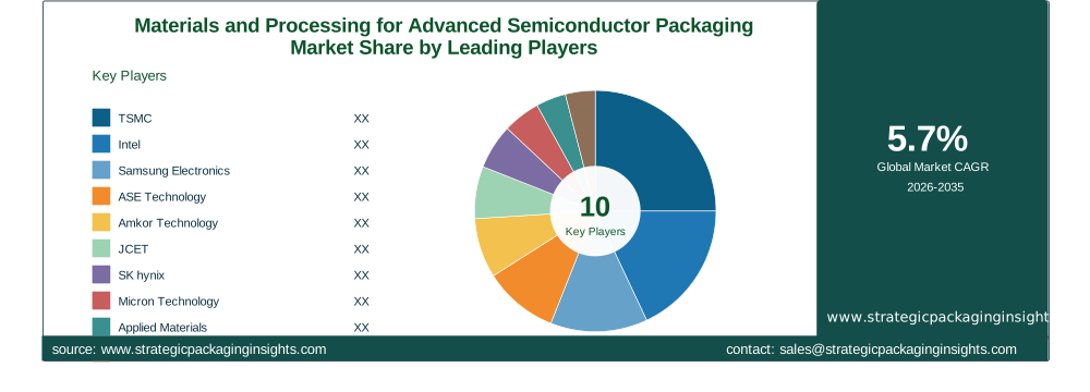
TSMC is a leading player in the market, known for its advanced packaging solutions and strong presence in the Asia Pacific region. The company has been investing heavily in R&D to develop innovative packaging technologies such as 3D IC and system-in-package. Intel is another major player, with a strong focus on developing high-performance packaging solutions for consumer electronics and data centers.
Samsung Electronics is also a key player in the market, with a strong presence in the semiconductor packaging industry. The company is known for its advanced packaging technologies and extensive manufacturing capabilities. Samsung is continuously expanding its production facilities to meet the growing demand for semiconductor packaging solutions.
Other notable players in the market include ASE Technology, Amkor Technology, and JCET, which are known for their expertise in advanced packaging technologies and strong customer relationships. These companies are focusing on expanding their product portfolios and enhancing their manufacturing capabilities to gain a competitive edge in the market.
Key Highlights
- Largest Region: Asia Pacific
- Fastest-Growing Region: Asia Pacific
- Largest Segment: Consumer Electronics
- Fastest-Growing Segment: High Performance Computing
- Base-year market size: USD $23 Billion
- Forecast-year market size: USD $40 Billion
- CAGR: 5.7%
- Important application: Consumer Electronics
- Major end-use industry: Automotive
- Major market driver: Demand for high-performance packaging solutions
Regional Insights
The global Materials and Processing for Advanced Semiconductor Packaging market is dominated by the Asia Pacific region, which is the largest and fastest-growing market. The region's growth is driven by the increasing demand for consumer electronics and high-performance computing applications. Countries like China, Japan, and South Korea are major contributors to the market, with significant investments in semiconductor manufacturing and packaging technologies.
North America
North America is a significant market for advanced semiconductor packaging, driven by the presence of major technology companies and a strong focus on innovation. The region is characterized by high demand for high-performance computing and data center applications. The U.S. is the largest contributor to the market, with significant investments in R&D and manufacturing capabilities.
The demand for advanced packaging solutions in North America is also driven by the growing adoption of AI and IoT technologies. Companies in the region are focusing on developing innovative packaging solutions to meet the evolving demands of these applications. The presence of major semiconductor companies like Intel and Applied Materials further strengthens the market in North America.
Europe
Europe is a growing market for advanced semiconductor packaging, with increasing demand for automotive and industrial electronics applications. The region is characterized by a strong focus on sustainability and environmental impact reduction, which is driving the adoption of eco-friendly packaging solutions. Germany and France are major contributors to the market, with significant investments in semiconductor manufacturing and packaging technologies.
The demand for advanced packaging solutions in Europe is also driven by the growing adoption of electric vehicles and smart devices. Companies in the region are focusing on developing innovative packaging solutions to meet the evolving demands of these applications. The presence of major semiconductor companies like Infineon and STMicroelectronics further strengthens the market in Europe.
Asia Pacific
The Asia Pacific region is the largest and fastest-growing market for advanced semiconductor packaging, driven by the increasing demand for consumer electronics and high-performance computing applications. Countries like China, Japan, and South Korea are major contributors to the market, with significant investments in semiconductor manufacturing and packaging technologies.
The demand for advanced packaging solutions in Asia Pacific is also driven by the growing adoption of AI and IoT technologies. Companies in the region are focusing on developing innovative packaging solutions to meet the evolving demands of these applications. The presence of major semiconductor companies like TSMC and Samsung Electronics further strengthens the market in Asia Pacific.
Latin America
Latin America is a growing market for advanced semiconductor packaging, with increasing demand for telecommunications and industrial electronics applications. The region is characterized by a strong focus on innovation and technology adoption, which is driving the demand for advanced packaging solutions. Brazil and Mexico are major contributors to the market, with significant investments in semiconductor manufacturing and packaging technologies.
The demand for advanced packaging solutions in Latin America is also driven by the growing adoption of AI and IoT technologies. Companies in the region are focusing on developing innovative packaging solutions to meet the evolving demands of these applications. The presence of major semiconductor companies like Intel and Samsung Electronics further strengthens the market in Latin America.
Middle East & Africa
The Middle East & Africa region is a growing market for advanced semiconductor packaging, with increasing demand for telecommunications and industrial electronics applications. The region is characterized by a strong focus on innovation and technology adoption, which is driving the demand for advanced packaging solutions. The UAE and South Africa are major contributors to the market, with significant investments in semiconductor manufacturing and packaging technologies.
The demand for advanced packaging solutions in the Middle East & Africa is also driven by the growing adoption of AI and IoT technologies. Companies in the region are focusing on developing innovative packaging solutions to meet the evolving demands of these applications. The presence of major semiconductor companies like Intel and Samsung Electronics further strengthens the market in the Middle East & Africa.
Materials and Processing for Advanced Semiconductor Packaging Market Segments Insights

By Material Type Analysis
The Materials and Processing for Advanced Semiconductor Packaging market is segmented by material type, with organic substrates, ceramic substrates, and silicon wafers being the most prominent materials. Organic substrates are widely used due to their cost-effectiveness and flexibility, making them suitable for a variety of applications. Ceramic substrates offer excellent thermal and electrical properties, making them ideal for high-performance applications. Silicon wafers are a critical component in semiconductor packaging, providing the foundation for advanced packaging technologies.
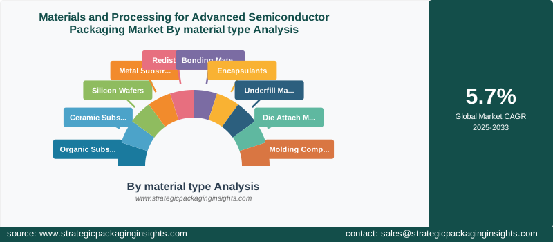
The demand for these materials is driven by the increasing need for high-performance and compact packaging solutions in consumer electronics and high-performance computing applications. Companies are focusing on developing advanced materials that offer improved performance and efficiency. The growing emphasis on sustainability is also driving the demand for eco-friendly materials in semiconductor packaging.
By Processing Technology Analysis
The market is also segmented by processing technology, with lithography, bonding and interconnection, and wafer processing being the most prominent technologies. Lithography is a critical process in semiconductor packaging, enabling the creation of intricate patterns on substrates. Bonding and interconnection technologies are essential for creating reliable connections between components, ensuring the performance and reliability of semiconductor packages.
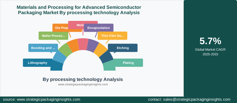
The demand for these processing technologies is driven by the increasing complexity of semiconductor packages and the need for higher performance and efficiency. Companies are investing in advanced processing technologies to meet the evolving demands of the market. The growing emphasis on automation and robotics in manufacturing processes is also driving the demand for advanced processing technologies in semiconductor packaging.
By Packaging Technology Analysis
The market is segmented by packaging technology, with flip chip, 3D IC packaging, and wafer-level packaging being the most prominent technologies. Flip chip technology offers significant advantages in terms of performance and space-saving, making it ideal for high-performance applications. 3D IC packaging is gaining traction due to its ability to integrate multiple components in a single package, offering enhanced performance and efficiency.
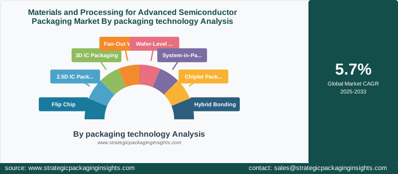
The demand for these packaging technologies is driven by the increasing need for high-performance and compact packaging solutions in consumer electronics and high-performance computing applications. Companies are focusing on developing innovative packaging technologies to meet the evolving demands of the market. The growing emphasis on sustainability is also driving the demand for eco-friendly packaging solutions in semiconductor packaging.
By Application Analysis
The market is segmented by application, with consumer electronics, data centers, and high-performance computing being the most prominent applications. Consumer electronics is the largest segment, driven by the increasing demand for smartphones, tablets, and other smart devices. Data centers and high-performance computing are also significant segments, driven by the growing need for advanced computing solutions in various industries.
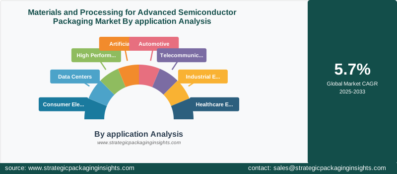
The demand for semiconductor packaging solutions in these applications is driven by the need for higher performance and efficiency. Companies are focusing on developing innovative packaging solutions to meet the evolving demands of these applications. The growing emphasis on sustainability is also driving the demand for eco-friendly packaging solutions in semiconductor packaging.
Materials and Processing for Advanced Semiconductor Packaging Market Segments
The Materials and Processing for Advanced Semiconductor Packaging market has been segmented on the basis ofBy material type
- Organic Substrates
- Ceramic Substrates
- Silicon Wafers
- Metal Substrates
- Redistribution Layer Materials
- Bonding Materials
- Encapsulants
- Underfill Materials
- Die Attach Materials
- Molding Compounds
By processing technology
- Lithography
- Bonding and Interconnection
- Wafer Processing
- Die Preparation
- Molding
- Encapsulation
- Thin Film Deposition
- Etching
- Plating
By packaging technology
- Flip Chip
- 2.5D IC Packaging
- 3D IC Packaging
- Fan-Out Wafer-Level Packaging
- Wafer-Level Packaging
- System-in-Package
- Chiplet Packaging
- Hybrid Bonding
By application
- Consumer Electronics
- Data Centers
- High Performance Computing
- Artificial Intelligence
- Automotive
- Telecommunications
- Industrial Electronics
- Healthcare Electronics
By region
- North America
- Europe
- Asia Pacific
- Latin America
- Middle East and Africa