Advanced Wafer Level Packaging Market Outlook
The Advanced Wafer Level Packaging market was valued at $7.23 billion in 2024 and is projected to reach $14.22 billion by 2033, growing at a CAGR of 7.80% during the forecast period 2025-2033. This market is experiencing significant growth due to the increasing demand for miniaturized electronic devices and the need for high-performance packaging solutions. The rise in consumer electronics, particularly smartphones and wearables, is driving the demand for advanced packaging technologies that offer enhanced performance and reduced size. Additionally, the automotive sector's shift towards electric and autonomous vehicles is further propelling the market, as these vehicles require sophisticated electronic systems that benefit from advanced wafer-level packaging.

Despite the promising growth, the market faces challenges such as high initial costs and complex manufacturing processes. Regulatory constraints and the need for significant capital investment can hinder market expansion. However, the potential for growth remains substantial, driven by technological advancements and the increasing adoption of IoT devices. The market is also witnessing a trend towards the integration of artificial intelligence and machine learning in packaging processes, which is expected to open new avenues for innovation and efficiency improvements. As companies continue to invest in research and development, the market is poised for robust growth, with opportunities for new entrants and established players alike.
Report Scope
| Attributes | Details |
| Report Title | Advanced Wafer Level Packaging Market Size, Future Growth and Forecast 2033 |
| Packaging Type | WLCSP, Fan-In WLP, Fan-Out WLP, eWLB |
| Application | Mobile, Wearables, Automotive, RF |
| Wafer Size | 200 mm, 300 mm, Others |
| End Use | OSATs, Foundries, IDMs, Fabless |
| Region | Asia Pacific, North America, Latin America, Europe, Middle East & Africa |
| Base Year | 2024 |
| Historic Period | 2017-2023 |
| Forecast Period | 2025-2033 |
| Number of Pages | 179 |
| Customization Available | Yes* |
Opportunities & Threats
The Advanced Wafer Level Packaging market presents numerous opportunities, particularly in the realm of consumer electronics. The proliferation of smartphones, tablets, and wearable devices is driving the demand for compact and efficient packaging solutions. As consumers continue to demand more functionality in smaller devices, manufacturers are compelled to adopt advanced packaging technologies that can accommodate these needs. Additionally, the rise of 5G technology is expected to further boost the market, as it requires sophisticated packaging solutions to support higher data rates and improved connectivity. The automotive industry also offers significant opportunities, with the increasing adoption of electric vehicles and autonomous driving technologies necessitating advanced electronic systems that rely on wafer-level packaging.
Another opportunity lies in the growing trend of IoT devices, which require efficient and reliable packaging solutions to ensure seamless connectivity and performance. As the number of connected devices continues to rise, the demand for advanced wafer-level packaging is expected to increase, providing ample growth opportunities for market players. Furthermore, the integration of AI and machine learning in packaging processes is anticipated to enhance efficiency and reduce costs, making advanced packaging solutions more accessible to a broader range of industries.
However, the market is not without its threats. One of the primary challenges is the high cost associated with advanced packaging technologies, which can be a barrier to entry for smaller companies. Additionally, the complexity of manufacturing processes and the need for specialized equipment can pose significant challenges. Regulatory constraints and the need for compliance with stringent industry standards can also hinder market growth. Despite these challenges, the market's potential for growth remains strong, driven by technological advancements and increasing demand across various industries.
Drivers & Challenges
The Advanced Wafer Level Packaging market is driven by several key factors, including the increasing demand for miniaturized electronic devices and the need for high-performance packaging solutions. The consumer electronics industry, in particular, is a major driver, with the proliferation of smartphones, tablets, and wearable devices necessitating advanced packaging technologies. Additionally, the automotive sector's shift towards electric and autonomous vehicles is further propelling the market, as these vehicles require sophisticated electronic systems that benefit from advanced wafer-level packaging. The rise of 5G technology is also expected to drive market growth, as it requires advanced packaging solutions to support higher data rates and improved connectivity.
Another significant driver is the growing trend of IoT devices, which require efficient and reliable packaging solutions to ensure seamless connectivity and performance. As the number of connected devices continues to rise, the demand for advanced wafer-level packaging is expected to increase, providing ample growth opportunities for market players. Furthermore, the integration of AI and machine learning in packaging processes is anticipated to enhance efficiency and reduce costs, making advanced packaging solutions more accessible to a broader range of industries.
Despite these drivers, the market faces several challenges that could hinder its growth. One of the primary challenges is the high cost associated with advanced packaging technologies, which can be a barrier to entry for smaller companies. Additionally, the complexity of manufacturing processes and the need for specialized equipment can pose significant challenges. Regulatory constraints and the need for compliance with stringent industry standards can also hinder market growth. However, with continued investment in research and development, these challenges can be mitigated, allowing the market to realize its full potential.
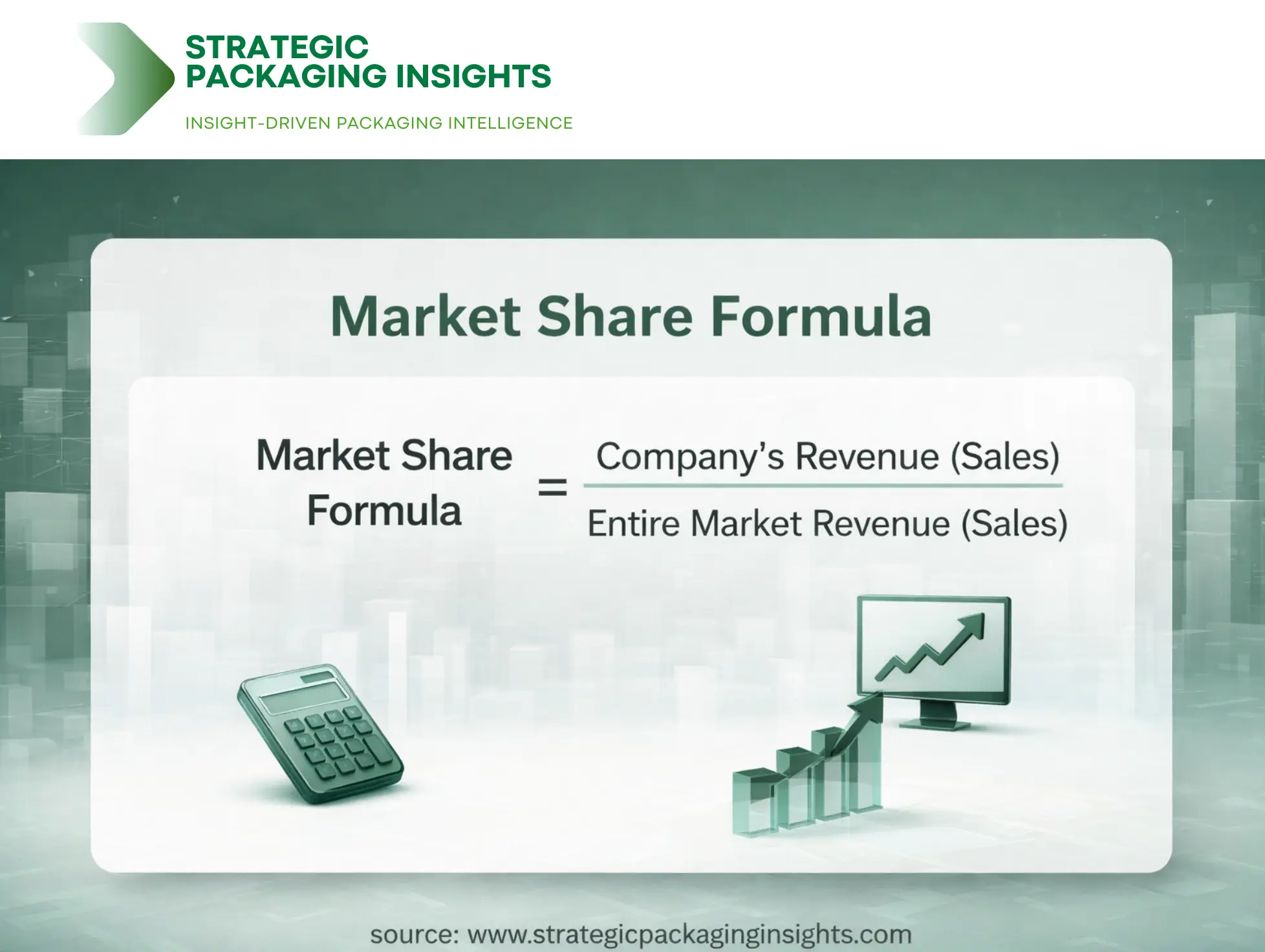
Market Share Analysis
The competitive landscape of the Advanced Wafer Level Packaging market is characterized by the presence of several key players who hold significant market shares. Companies such as ASE Technology, Amkor Technology, TSMC, Samsung Electronics, and Intel are among the leading players in the market, each contributing to the market's growth through innovation and strategic partnerships. These companies have established themselves as leaders in the industry by investing heavily in research and development to enhance their product offerings and maintain a competitive edge.

ASE Technology is a prominent player in the market, known for its comprehensive range of packaging solutions and strong focus on innovation. The company has a significant market share, driven by its extensive experience and expertise in the field. Amkor Technology is another major player, recognized for its advanced packaging technologies and commitment to quality. The company's strong global presence and strategic partnerships have enabled it to maintain a competitive position in the market.
TSMC, a leading semiconductor foundry, plays a crucial role in the market by providing advanced packaging solutions to a wide range of industries. The company's focus on innovation and technological advancements has helped it secure a significant market share. Samsung Electronics, a global leader in electronics, is also a key player in the market, offering a diverse range of packaging solutions that cater to various industries. The company's strong brand reputation and extensive distribution network have contributed to its success in the market.
Intel, a renowned technology company, is another major player in the Advanced Wafer Level Packaging market. The company's focus on research and development and its commitment to delivering high-quality products have helped it maintain a strong market position. Other notable companies in the market include JCET Group, SPIL, Powertech Technology, Nepes, and Chipbond Technology, each contributing to the market's growth through their unique offerings and strategic initiatives.
Key Highlights
- The Advanced Wafer Level Packaging market is projected to grow at a CAGR of 7.80% from 2025 to 2033.
- Key drivers include the demand for miniaturized electronic devices and the rise of 5G technology.
- Challenges include high costs and complex manufacturing processes.
- Opportunities exist in the consumer electronics and automotive industries.
- Key players include ASE Technology, Amkor Technology, TSMC, Samsung Electronics, and Intel.
- The market is witnessing a trend towards the integration of AI and machine learning in packaging processes.
- Regulatory constraints and the need for compliance with industry standards pose challenges.
Top Countries Insights
In the Advanced Wafer Level Packaging market, the United States holds a significant position, with a market size of approximately $2.5 billion and a CAGR of 6%. The country's strong presence in the semiconductor industry and the increasing demand for advanced packaging solutions in consumer electronics and automotive sectors are key growth drivers. Government initiatives to promote technological advancements and innovation further support market growth. However, challenges such as high manufacturing costs and regulatory constraints remain.

China is another major player in the market, with a market size of around $3 billion and a CAGR of 9%. The country's robust electronics manufacturing industry and the growing demand for smartphones and other consumer electronics drive the market. Additionally, government policies supporting the semiconductor industry and investments in research and development contribute to market growth. However, the market faces challenges such as intellectual property issues and competition from other countries.
Germany, with a market size of $1.2 billion and a CAGR of 5%, is a key player in the European market. The country's strong automotive industry and the increasing adoption of electric vehicles drive the demand for advanced packaging solutions. Government initiatives to promote sustainable technologies and innovation further support market growth. However, challenges such as high production costs and regulatory constraints remain.
Japan, with a market size of $1 billion and a CAGR of 4%, is a significant player in the Asia Pacific region. The country's advanced technology sector and the growing demand for consumer electronics drive the market. Government support for technological advancements and innovation further contributes to market growth. However, challenges such as high manufacturing costs and competition from other countries remain.
South Korea, with a market size of $800 million and a CAGR of 7%, is another key player in the market. The country's strong semiconductor industry and the increasing demand for advanced packaging solutions in consumer electronics and automotive sectors drive the market. Government initiatives to promote innovation and technological advancements further support market growth. However, challenges such as regulatory constraints and competition from other countries remain.
Advanced Wafer Level Packaging Market Segments Insights

Packaging Type Analysis
The Packaging Type segment in the Advanced Wafer Level Packaging market is crucial, with sub-segments including WLCSP, Fan-In WLP, Fan-Out WLP, and eWLB. WLCSP is gaining traction due to its cost-effectiveness and ability to support high-volume production, making it ideal for consumer electronics. Fan-In WLP is favored for its compact design and reliability, particularly in mobile and wearable applications. Fan-Out WLP offers enhanced performance and flexibility, making it suitable for high-performance applications such as automotive and RF. eWLB is recognized for its ability to support complex designs and high-density interconnections, catering to advanced applications in various industries.

Each sub-segment is driven by specific industry demands and technological advancements. WLCSP's growth is fueled by the increasing demand for miniaturized devices, while Fan-In WLP benefits from the need for reliable and compact packaging solutions. Fan-Out WLP's flexibility and performance advantages drive its adoption in high-performance applications, while eWLB's ability to support complex designs makes it a preferred choice for advanced applications. The competitive landscape in this segment is characterized by innovation and strategic partnerships, with companies investing in research and development to enhance their offerings and maintain a competitive edge.
Application Analysis
The Application segment in the Advanced Wafer Level Packaging market includes Mobile, Wearables, Automotive, and RF. The Mobile sub-segment is a major driver, with the proliferation of smartphones and tablets necessitating advanced packaging solutions that offer enhanced performance and reduced size. Wearables are also driving demand, as consumers seek compact and efficient devices with extended battery life. The Automotive sub-segment is experiencing significant growth, driven by the increasing adoption of electric vehicles and autonomous driving technologies that require sophisticated electronic systems.

RF applications are gaining traction due to the rise of 5G technology, which requires advanced packaging solutions to support higher data rates and improved connectivity. Each sub-segment is characterized by specific industry demands and technological advancements, with companies investing in research and development to enhance their offerings and maintain a competitive edge. The competitive landscape in this segment is marked by innovation and strategic partnerships, with companies seeking to capitalize on the growing demand for advanced packaging solutions across various industries.
Wafer Size Analysis
The Wafer Size segment in the Advanced Wafer Level Packaging market includes 200 mm, 300 mm, and Others. The 200 mm sub-segment is driven by the demand for cost-effective solutions in consumer electronics and other high-volume applications. The 300 mm sub-segment is gaining traction due to its ability to support high-performance applications and advanced technologies, making it suitable for industries such as automotive and RF. The Others sub-segment includes various wafer sizes that cater to specific industry needs and applications.

Each sub-segment is characterized by specific industry demands and technological advancements, with companies investing in research and development to enhance their offerings and maintain a competitive edge. The competitive landscape in this segment is marked by innovation and strategic partnerships, with companies seeking to capitalize on the growing demand for advanced packaging solutions across various industries. The market is witnessing a trend towards larger wafer sizes, driven by the need for enhanced performance and efficiency in high-performance applications.
End Use Analysis
The End Use segment in the Advanced Wafer Level Packaging market includes OSATs, Foundries, IDMs, and Fabless. OSATs are a major driver, providing outsourced packaging solutions to a wide range of industries. Foundries play a crucial role in the market, offering advanced packaging solutions to semiconductor companies and other industries. IDMs are also significant players, providing integrated solutions that combine design, manufacturing, and packaging capabilities.

Fabless companies are gaining traction, driven by the increasing demand for specialized packaging solutions that cater to specific industry needs. Each sub-segment is characterized by specific industry demands and technological advancements, with companies investing in research and development to enhance their offerings and maintain a competitive edge. The competitive landscape in this segment is marked by innovation and strategic partnerships, with companies seeking to capitalize on the growing demand for advanced packaging solutions across various industries.
Advanced Wafer Level Packaging Market Segments
The Advanced Wafer Level Packaging market has been segmented on the basis ofPackaging Type
- WLCSP
- Fan-In WLP
- Fan-Out WLP
- eWLB
Application
- Mobile
- Wearables
- Automotive
- RF
Wafer Size
- 200 mm
- 300 mm
- Others
End Use
- OSATs
- Foundries
- IDMs
- Fabless
Region
- Asia Pacific
- North America
- Latin America
- Europe
- Middle East & Africa