
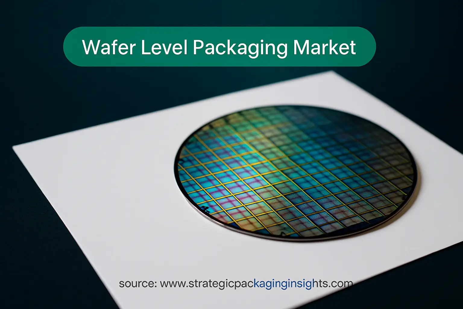
Explore the Wafer Level Packaging Market's growth trajectory, segment insights, regional dynamics, and the balance of challenges and opportunities shaping its future.
Why This Market Is Gaining Attention
The Wafer Level Packaging Market is capturing significant attention due to its pivotal role in advancing semiconductor technology. As the demand for miniaturized and high-performance electronic devices surges, wafer level packaging (WLP) offers a solution that enhances device performance while reducing size and cost. This market is becoming increasingly critical as industries such as consumer electronics, automotive, and telecommunications seek more efficient and compact packaging solutions to meet the growing technological demands.
https://www.strategicpackaginginsights.com/report/wafer-level-packaging-market
Market Scale & Growth Momentum
The Wafer Level Packaging Market is poised for robust growth, with its market size expected to expand from $10.09 billion in 2025 to $26.44 billion by 2034. This impressive growth trajectory, marked by a compound annual growth rate (CAGR) of 11.3%, underscores the increasing adoption of WLP technologies across various sectors. The market's expansion is driven by the escalating need for advanced packaging solutions that support the integration of more functionalities into smaller chip sizes, thereby enhancing the overall performance and efficiency of electronic devices.
Deep Dive into Segments
| Segment | Description |
|---|---|
| By Packaging Type | Fan-in WLP, fan-out WLP, and 2.5D/3D packaging are the primary types. Fan-in WLP is popular for its cost-effectiveness in small devices, while fan-out WLP offers more space for interconnects, crucial for high-performance applications. 2.5D/3D packaging is gaining traction for its ability to stack chips, enhancing performance and reducing latency. |
| By Technology | Technologies such as Redistribution Layer (RDL), Through-Silicon Via (TSV), and bumping are integral. RDL is essential for rerouting connections, TSV enables vertical stacking of chips, and bumping is critical for creating reliable interconnections. |
| By Application | Consumer electronics, automotive, telecom, and sensors are key applications. Consumer electronics dominate due to the high demand for compact and efficient devices. Automotive applications are growing with the rise of autonomous vehicles requiring advanced sensors and processing capabilities. |
| By End Use | Semiconductor foundries, Outsourced Semiconductor Assembly and Test (OSATs), and electronics OEMs are the main end-users. Foundries and OSATs are crucial for manufacturing and testing, while OEMs drive demand through product innovation. |
| Region | Asia Pacific, North America, Latin America, Europe, and Middle East & Africa. Asia Pacific leads due to its strong semiconductor manufacturing base, while North America and Europe are significant due to technological advancements and high R&D investments. |
Application & End-Use Relevance
The relevance of wafer level packaging extends across multiple applications and end-use sectors. In consumer electronics, WLP is essential for developing smaller, more efficient devices such as smartphones and tablets. The automotive industry benefits from WLP through enhanced sensor integration and processing capabilities, crucial for the development of autonomous and electric vehicles. In telecommunications, WLP supports the miniaturization and performance enhancement of network infrastructure components. Semiconductor foundries and OSATs are pivotal in the production and testing phases, ensuring that the packaged chips meet the required standards and performance metrics.
Regional & Industry Dynamics
Regionally, the Asia Pacific dominates the Wafer Level Packaging Market, driven by its robust semiconductor manufacturing industry and the presence of major electronics manufacturers. North America and Europe are also significant players, with a focus on innovation and technological advancements. These regions invest heavily in research and development, fostering the growth of advanced packaging technologies. Latin America and the Middle East & Africa are emerging markets, with increasing investments in semiconductor infrastructure and technology adoption.
Challenges vs Opportunities
The Wafer Level Packaging Market faces several challenges, including the high cost of advanced packaging technologies and the complexity of integrating multiple functionalities into a single package. However, these challenges are counterbalanced by opportunities such as the growing demand for miniaturized devices, advancements in IoT and AI technologies, and the increasing adoption of electric and autonomous vehicles. The market's ability to innovate and adapt to these trends will be crucial in overcoming the existing challenges and capitalizing on the opportunities.
SWOT Overview
| Strengths | Weaknesses | Opportunities | Threats |
|---|---|---|---|
| High demand for miniaturization | High initial investment costs | Growth in IoT and AI applications | Rapid technological changes |
| Advanced performance capabilities | Complex manufacturing processes | Expansion in automotive electronics | Intense competition |
| Strong industry partnerships | Limited skilled workforce | Emerging markets in Latin America | Economic fluctuations |
Innovation & Sustainability Angle
Innovation in the Wafer Level Packaging Market is centered around enhancing performance while reducing environmental impact. Companies are investing in sustainable manufacturing processes and materials to minimize waste and energy consumption. The development of eco-friendly packaging solutions is becoming a priority, driven by regulatory pressures and consumer demand for sustainable products. Innovations such as the use of biodegradable materials and energy-efficient production techniques are setting new standards in the industry.
What This Means for Packaging Stakeholders
For stakeholders in the Wafer Level Packaging Market, the current trends and future prospects present both challenges and opportunities. Manufacturers must focus on innovation and sustainability to remain competitive, while also addressing the cost and complexity challenges associated with advanced packaging technologies. Collaboration across the supply chain, from material suppliers to end-users, will be essential in driving growth and meeting the evolving demands of the market. As the industry continues to evolve, stakeholders who can adapt to the changing landscape and leverage new technologies will be well-positioned to capitalize on the market's growth potential.